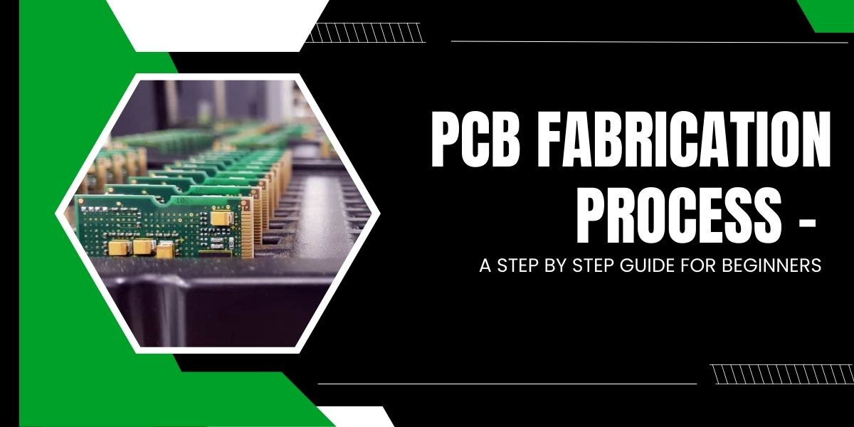
PCB fabrication is a detail-intensive process, and even simple mistakes can cost businesses through faulty construction. When choosing your PCB fabrication company, consider using PCB fabricators with a demonstrated record of success
1. Designing the PCB board :
If a PCB is the foundation of an electronic device, the design is the foundation of the PCB. No matter how experienced the manufacturing staff may be, proceeding to the PCB fabrication process without laying out a clear and detailed design is an invitation to failure.
2. Cutting Base Laminate :
Once the design is ready, the PCB fabrication process officially begins. It starts with the cutting of the base copper-clad laminates into small pieces which is more convenient in production. PCBs can be single-layered, dual-layered or multi-layered, but all the base laminates are substrate with one layer or two layers of copper sheet.
3. Copper Pattern Printing
The design defining the pathway and layout of circuits is then printed on the laminated board. All the steps are to be followed with a knack of precision because small negligence at any step can lead to the failure of the entire circuit. So this is a very critical PCB board fabrication process.
4. Etching :
Etching refers to the removal of excess copper. Once the pathway is printed on the board, it is covered to prevent exposure to the copper-removing chemical. Here, you must note that several rounds of testing and inspection are conducted throughout the PCB board fabrication process to ensure that every step is carried out well.
5. Lamination and Pressing
At this step, all the layers are stacked up and laminated together by heating them at a high temperature and applying pressure by machines. Punch holes are used to align all the layers. While machines carry out many of the steps of the PCB fabrication process, certified technicians are required to monitor the process at every stage.
6. Drilling Holes
After locating the drill spots using an X-ray machine, they are drilled using a computer-guided process. This is necessary to expose the inner layers. A copper layer is deposited on these freshly drilled holes.
7. Plating and Etching :
Yes, etching has been mentioned before, but a final etching is required before a PCB can be sent further for assembly. So, unwanted copper is again removed using chemical washes in this step. Via holes, copper plating is extremely important in the PCB fabrication process because all the traces are connected through these small drills.
8. Solder Mask Printing
The typical green color of PCBs is obtained thanks to this step. The PCB board fabrication process includes a step where a protective coating is added to the surface. This step is called solder mask application.
9. Silkscreen Printing
This is one of the crucial steps in the PCB fabrication process. This includes the printing of essential signs and markings on the surface of the circuit board. Logos, reference numbers, polarity indicators and other such markings are printed in this step.
10. Surface Finishes
In this process, a thin layer of metal will be applied to the copper pads which are not covered by a solder mask. This step is necessary to prevent the pads from oxidation. It gives a final finishing touch to the pads on the PCB board and helps enhance its quality in PCB assembly.
11. Testing and Inspection
While several rounds of testing and inspection are conducted throughout the PCB fabrication process, a final round is essential before sending the PCB further for assembly. Without performing this step, the PCBs cannot be passed for further use. If you need further assistance in selecting the right PCB manufacturer In India or have any specific questions about your PCB projects

 August 28, 2024 - BY Admin